Thinking Outside of the Box with 3D Printing: Optimizing the Programming Process
- Nov 17, 2016
- 3 min read
We recently wrote a blog article about how 3D printers help in the manufacturing process of PCB boards. The following article demonstrates just one way in which 3D Printing can make PCB programming more efficient while also making it easier to miniaturize components. This is also a great example for how 3D printing can be used for problem-solving in education by teaching students to think outside of the box so they are always looking for ways to improve upon existing procedures. 3D printing is not only a vital tool to those in engineering fields, but can also assist in any discipline requiring precision such as chemistry or architecture. To read more about 3D printing in educational institutions and why it is imperative for students to learn this technology, please visit this link. To follow along with our example of how we used 3D printing to innovate programming, keep reading!

This particular PCB that we are working with contains a motion sensor, (as depicted above) and is commonly found in wearable technology such as smartwatches and fitness monitors.

This motion sensor is one of the tracking mechanisms these wearables employ and is an integral part of the functionality of each device. To use a sensor PCB like this one in a wearable, there will be obvious size restrictions, so engineers and students have to think of innovative ways to get around them.
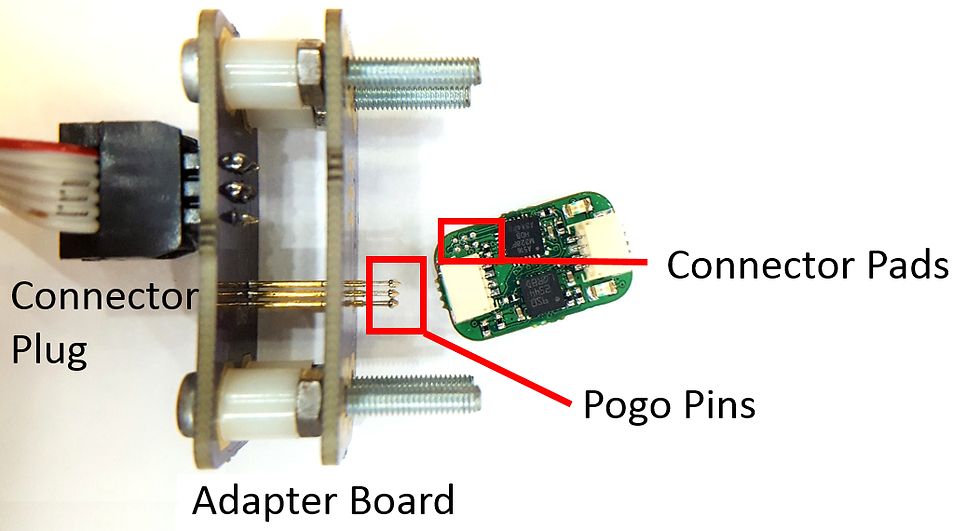
Typically when using PCBs, large connector pins are required to make contact with the pins of the microcontroller shown below in order to be able to program the PCB's micrcontroller.

A microcontroller is essentially what you plug in to your computer in order to program the specific board to do something. The ability to connect and program the microcontroller is crucial (your PCB would be useless without the program!) but traditionally can take up a lot of unnecessary space on your board.
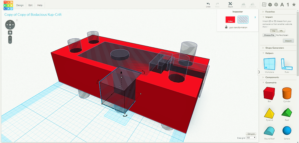
With regular connector pins, the connector plug would be easy to connect, and too much space would be taken up on the PCB itself to house these pins, resulting in the need for a larger PCB to include all necessary components. In the following case, we needed to keep our PCB very small so we devised a simple way to use tiny connector pads instead of the standard connector pins to save space. We also designed an adapter board that turns the connector plug into an array of tiny pogo pins. The challenge in using these pads is that they need to perfectly align with the pogo pins of the external programmer (which is the connecting point between your computer and your PCB) which can not be done reliably without a guide of some sort, so we employed the knowledge we have about 3D printing and design to create a custom 3D printed PCB guide that took us only about 30 minutes to make, from initial design to actual printout.

You can create your own design by using your preferred CAD software or the free 3D modeling software TinkerCAD. If you do not know how to 3D model, you can learn how by clicking here. Once finished, simply send the file wirelessly to your ZEUS to be printed out!

To print our PCB guide, we used the slicer onboard ZEUS to add brim layers to guarantee precision and chose the highest 80 micron resolution setting for the smoothest finish. If you are unfamiliar with these terms, please click here.

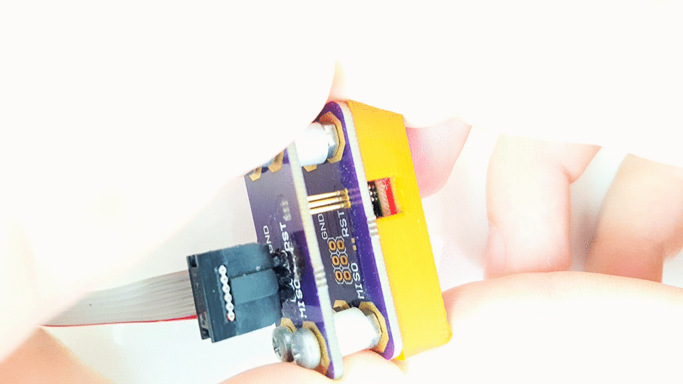
The design of the PCB guide can be quickly and easily reiterated, with each iteration taking under 20 minutes to have a physical product. This way, the alignment of the pogo pins and programming pads can be optimized in the sub-millimeter space, guaranteeing an accurate connection between the programmer and the PCB.


Once the perfect fit of the PCB in the PCB guide is achieved, the motion sensor can be tested by running a demo program on the PCB.

Extra: Customized PCB holder for testing multiple PCBs
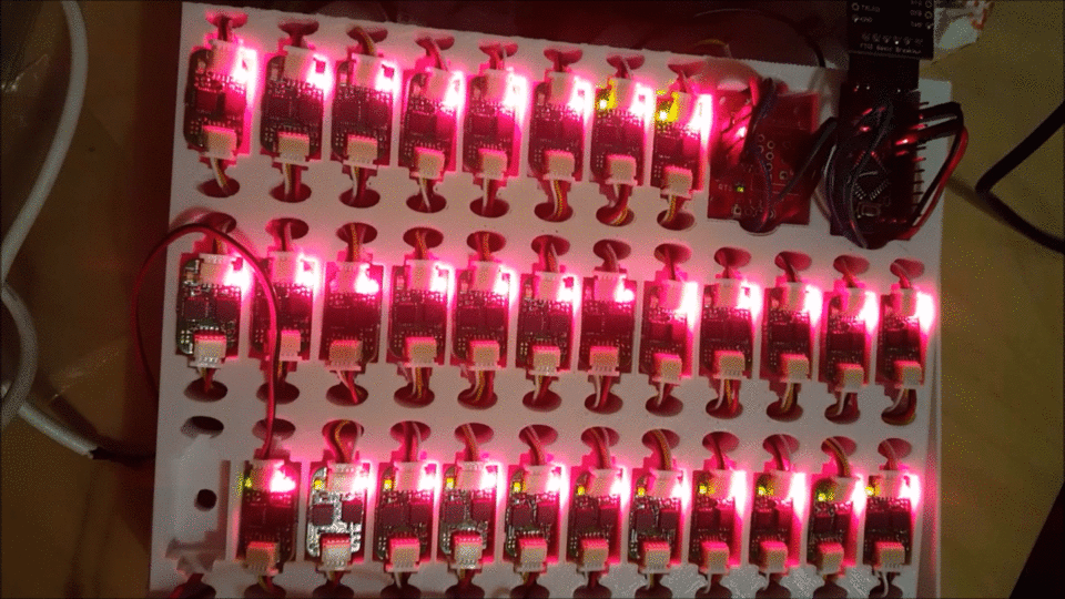
To test many PCBs at once, we built a large rig capable of holding multiple PCBs. This large testing rig was also designed in TinkerCAD and printed on ZEUS.


Once printed, the PCBs can be inserted and tested.


Comments