
3D Printing Fixtures for PCB Manufacturing
- Oct 4, 2016
- 2 min read
During the development of a Printed Circuit Board (PCB), the ZEUS 3D Printer can be a handy tool to ensure high quality in the manufacturing process. Learn how the ZEUS 3D Printer assisted in the design of these tiny sensor modules.
1) Manufacturing the PCB
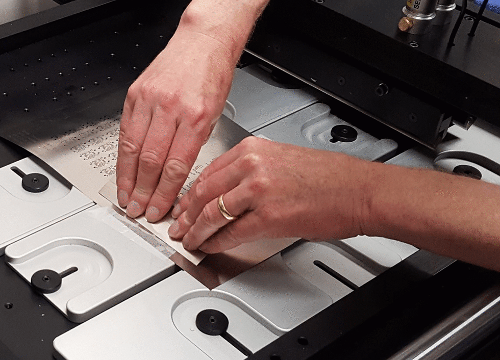
Assembling a PCB with two sides can be tricky. A fixture to stabilize the board and minimize deformation of the board is needed in the process where soldering paste is applied on the PCB contact pins to solder the electronic components (ICs, resistors, capacitors, etc.). It is relatively easy to apply soldering paste on one side of the PCB (with a flat bottom). However, once the first side of the PCB is assembled, trying to proceed with the other side can be tricky. Without a proper fixture to stabilize the bottom, soldering paste can not be applied to the board because the PCB can bend and lead to a misalignment of the stencil that keeps the soldering paste in place. If the soldering paste is not aligned properly on the PCB contact pins, complications in the later manufacturing steps with arise (Pick & Place, Soldering), resulting in poor quality of the PCB.
Solution? --> 3D Printing a fixture to support the PCB from the bottom during stenciling. This process to design and print the fixture took less than 1h with the ZEUS 3D Printer. The following steps were accomplished:
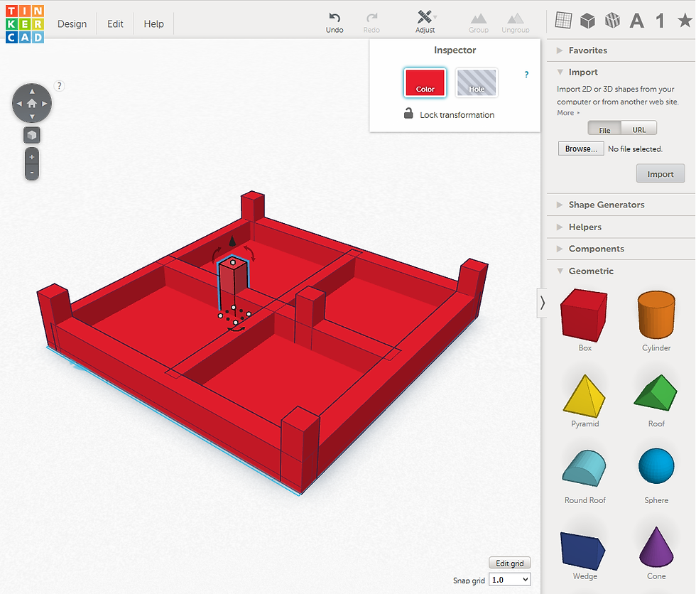
Step 1: Open Tinkercad (free browser software to model 3D files) and create a 3D model of the desired fixture.
2) Export the fixture as a 3D Printing File (STL) and send it to ZEUS for 3D Printing.

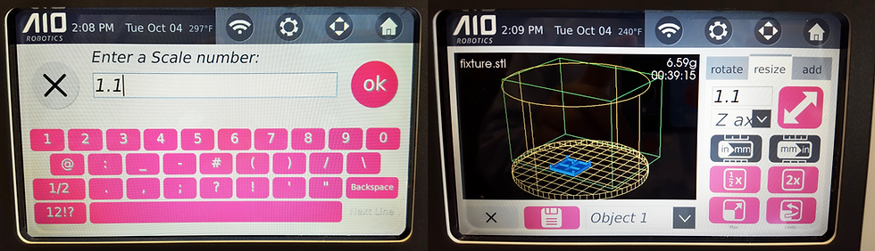
To print multiple iterations with different fixture heights, you can use the scale functionality on-board of ZEUS to easily scale along the Z-axis and adjust the height of your fixture. This is a convenient tool if you wish to do small changes or create multiple versions of the fixture.
For quick resolution prints, the fixture print takes roughly 10 minutes. For high-resolution prints, expect 25 minutes.

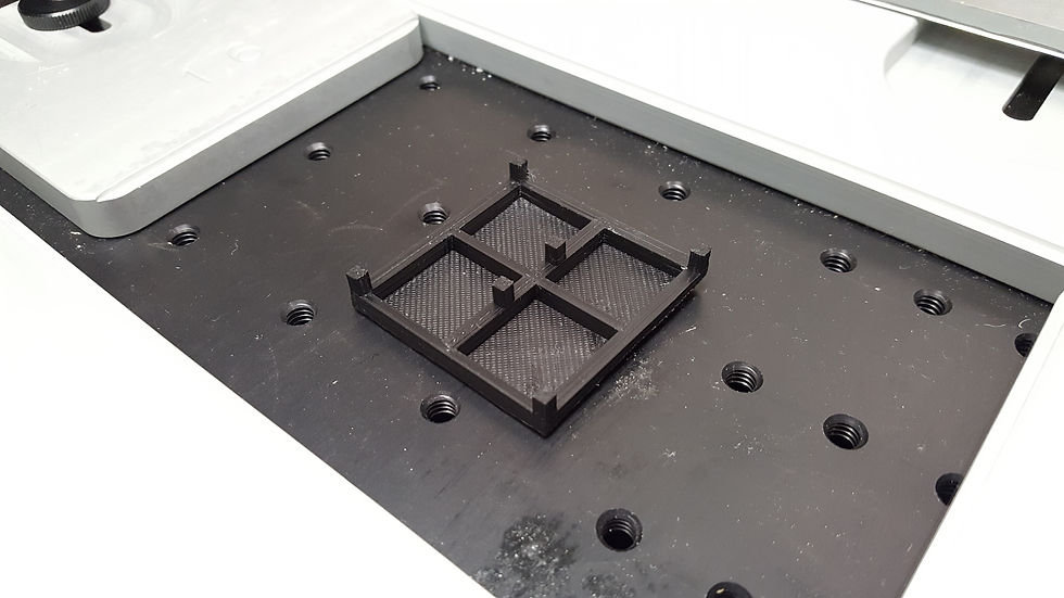
3) After the print is done, place the fixture on the stenciling table.
3) Align the non-assembled PCB side on the stenciling table facing up.

4) The bottom side of the PCB will be stabilized by the fixture and is used as a support when pushing the soldering paste over upper side of the PCB.

5) A stencil is placed on top of the PCB board and allows the soldering paste to only get applied on the contact pins on which the electronic components will be placed later.


6) The fixture allows to put pressure on top of the PCB when pushing soldering paste over the stencil.
7) Now the PCB is placed into a Pick&Place machine. The PCB will be assembled with electronic components and put in the oven for soldering. After this process the PCB manufacturing is accomplished and we move forward to the PCB testing.
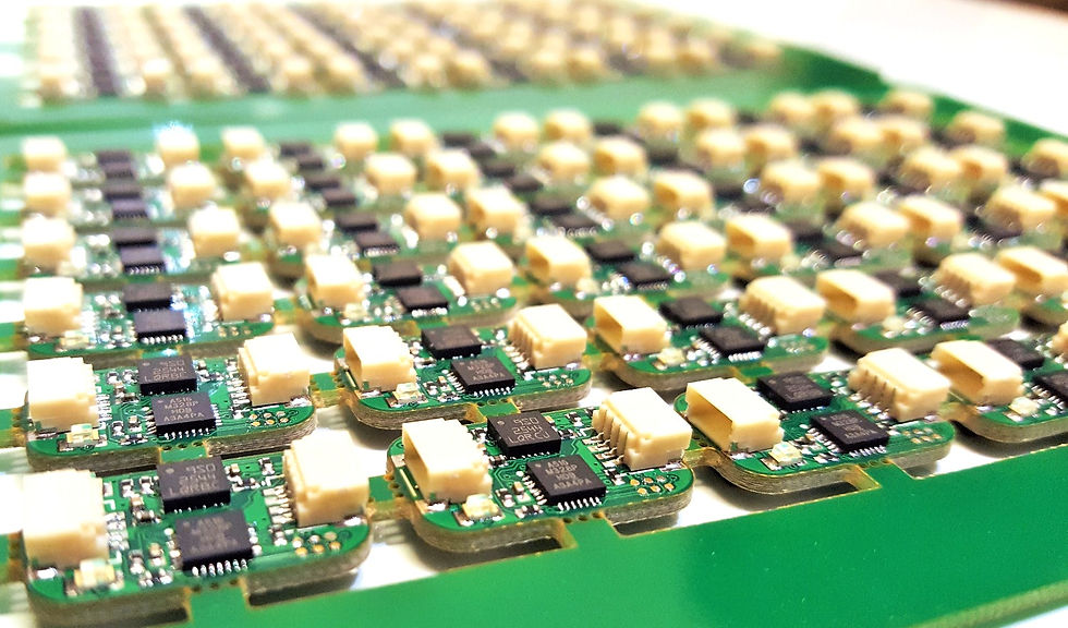
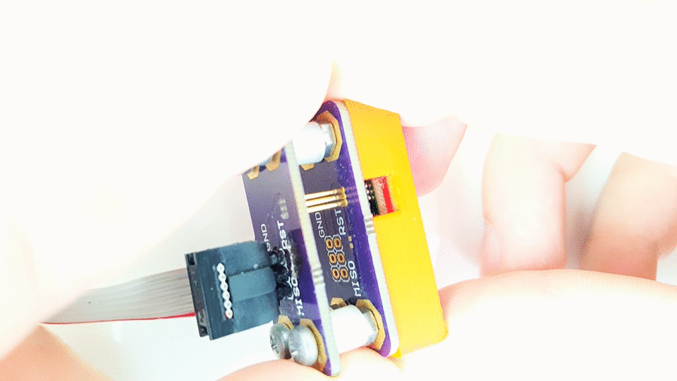
8) The sensor modules are ready and can be used and programmed. Here is a close picture of a single sensor module.


Comments